STATE-OF-THE-ART
The R&D-platform InnovationLab offers cutting-edge infrastructure and profound know-how for the development of novel products from lab scale to industrial scale.
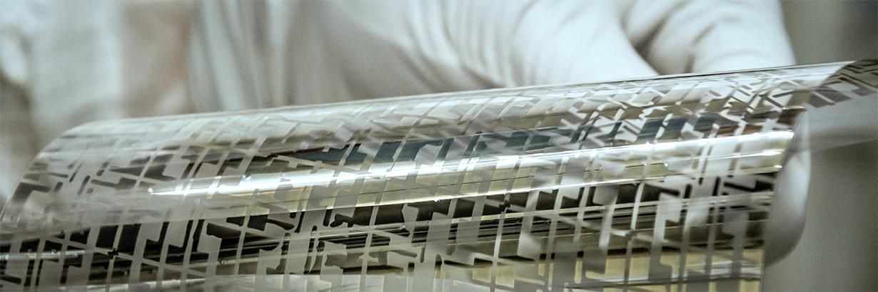
Equipment for Printed and Organic Electronics
Together with our partners from academia and industry we are offering a research platform with a broad infrastructure for research and development of printed and organic electronics. This interdisciplinary
collaboration enables acces to a versatile equipment park.
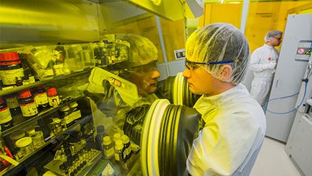
On a total of 6200 m², from office spaces tolaboratories and cleanrooms, you can benefit from a unique compilation of state-of-the-art research infrastructure such as an integrated UHV-system with FIB, SEM, XPS, FTIR and more for the in situ-analysis. In addition, our equipment includes characterization tools such as a climatic chamber, force/displacement measurement, drop shape analysis system, or rheometer and infrastructure such as glove boxes, exhaust hoods and a yellow room for lithography. Our all-u-can-use-flatrate package futher includes various types of printing presses from laboratory scale to pilot plants and industrial production - all under one roof.
Oberflächenanalytik
Clustertool = Ultra high vacuum system for investigation of organic thin-film layer systems without breaking vacuum and critical sample transfers.
- vacuum evaporation
- solution processing (spin-coater)
- dry nitrogen glovebox
- Auriga® CrossBeam® - Workstation (SEM, FIB, GIS)
- Physical Electronics PHI 5000 VersaProbe (XPS, UPS, IPES)
- Bruker Vertex 80v (FTIR-Spectrometer)
- DME BRR scanning probe microscopy (AFM, STM, SKP)
Printing and Coating
Printing, Coating & Surface Treatment
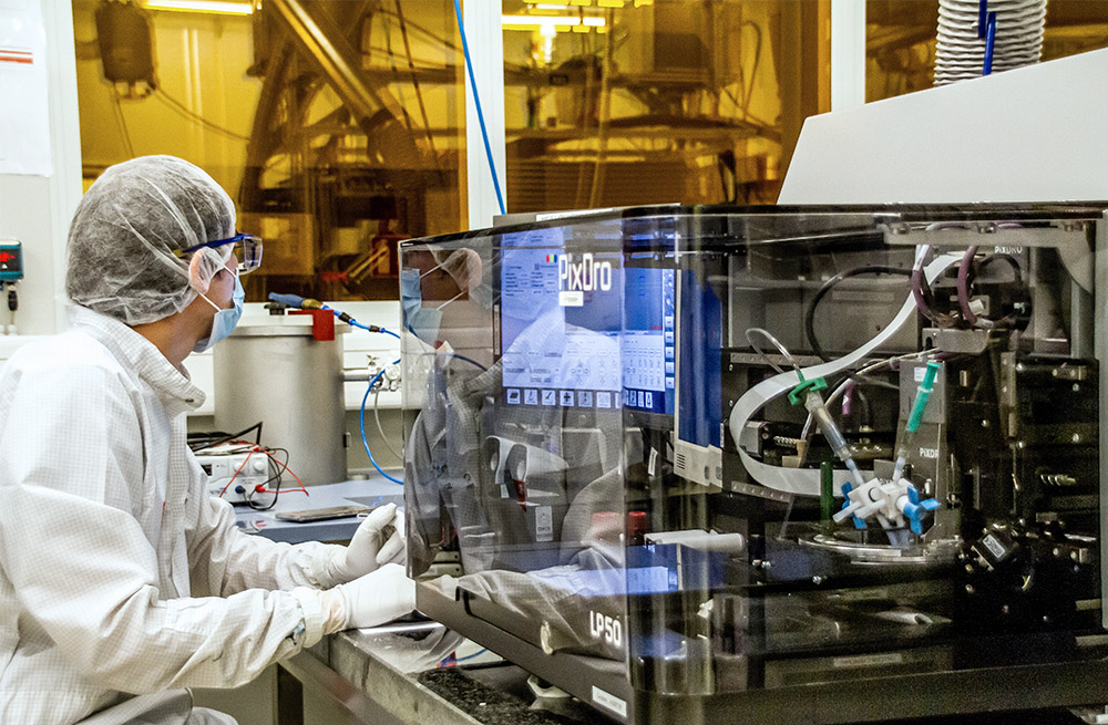
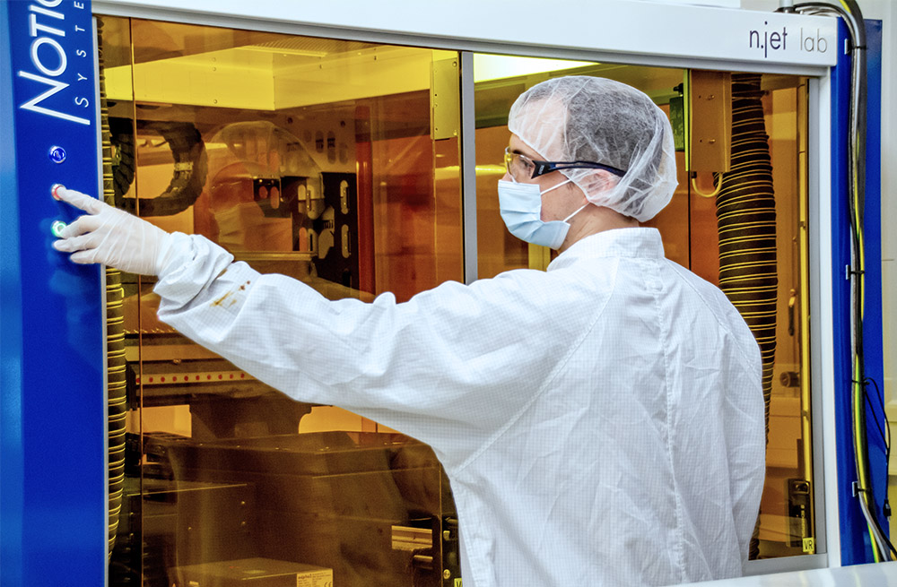
- inkjet printing (Dimatix, PixDro, n.jet hybrid)
- blade-coating (Ericson coatmaster)
- screen printing (Thieme), up to 580 x 750 mm²
- aerosol jet (Optomec)
- spin-coating
- thermal transfer printing (Zebra)
- 3D printers
- plasma/UV treatment
- temperature and vacuum hardening
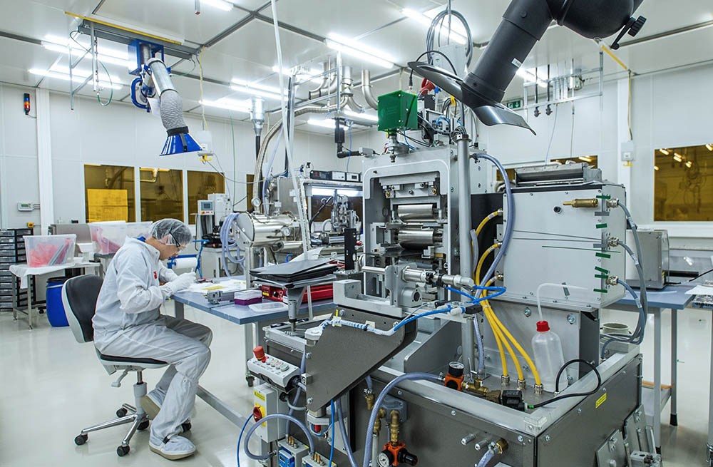
Roll-2-Roll Printing Press for Prototyping and Industrial Production
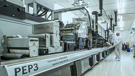
PEP3 (based on Gallus RCS 330)
- printing and drying of single or multilayer functional material systems
- large volume manufacturing capabilities
- substrate size up to 330 x 609 mm
designs up to several meters in length available upon request - Depending on the printing process, tests can be carried out starting already from 100 ml ink consumption via special adjustments
- pretreatment
- printing processes: flexo, gravure, screen and offset printing
- optional: inkjet printing
- drying: UV, IR, convection and active cooling
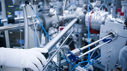
PVD, CVD and Photolithography
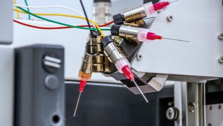
Evaporation System HHV (Edwards)
- metals:gold, silver, aluminium, titanium, etc.
Parylene Coater PDS 2010E (Specialty Coating Systems Inc.)
- complete encapsulation of components
- production of dielectric layers in OFETs
- materials: parylene C/-N or A-174 silane
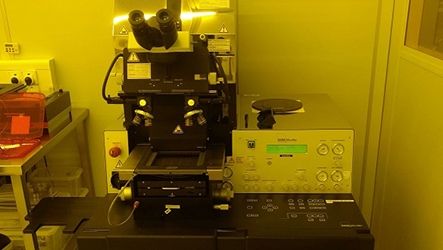
Suss MicroTec Mask Aligner:
- mask frame: 7” masks & 5” masks
- to be used for MEMS applications, production of optical components and compound semiconductors
Wet Bench:
- 4x Heated Ultrasonic Bath (3x suitable for flammable liquids)
- 3x QDR sinks (Quick Dump Rinse)
- fully equipped with Filter-Fan Units
Inertgas-Systems
Multiple Glove Boxes:
- nitrogen atmosphere
- designed for handling solvents
- spin-coating
- systems for thermal evaporation: metals, salts, organic materials
- IV-, LIV-, SMU- and spectral characterization
- UV-curing
Further Laboratory Equipment: ultrasonic bath, heating panels
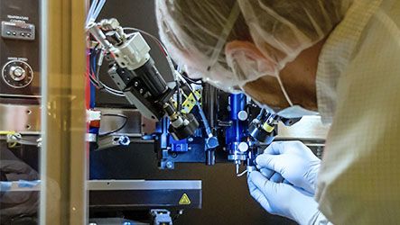
Further Thin Film and Material Characterization Methods
White-Light Interferometer Sensofar (Newport)
- suitable for the characterization of thin films
- measurable heights between some nm up to 1 cm
Surface Profilometers Dektak 150 (Veeco Instruments)
- large Z-range of 1 millimeter
- vertical resolution: 1Å max.

Ambient Atomic Force Microscope Scanner DualScope™ 95 50 (DME)
- scanning area: 50 µm x 50 µm x 5 µm
- possibility for electrical measurements such as KPFM
Kelvin Probe KP020 (KP Technology)
- high quality measurements of work function/fermi level
- resolution of work function: 1 - 3 meV
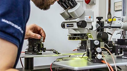
Various optical microscopes
Ellipsometer SENpro (Sentech)
- determination of layer thickness and optical constants (single and multilayer films)
- spectral area: 370 nm up to 1050 nm
UV-Vis-Spectrometer DH-S-BAL (Avantes)
- simple absorption and transmission spectroscopy from 200-2500 nm
Methods for Ink Characterization
- Contact angle/surface tension measuring system DSA100 (Krüss)
- rheometer (Haake Mars)