ANALYTICS
We investigate chemical and electronic material properties of organic semiconductor surfaces and interfaces by photoemission spectroscopy.
TU Darmstadt (MaWi) - Analytic
The Surface Science Laboratory of Technical University Darmstadt at InnovationLab is part of the Competence Center Analytics. Here, we work in strong cooperation with the research groups of Heidelberg University and Technical University Braunschweig.
Our research at iL mainly focuses on chemical and electronic properties of surfaces and interfaces of organic semiconductor systems. We particularly work on
- doping mechanisms,
- defined modification of interface contact properties,
- correlation of electronic materials and electric device properties of OLEDs, and
- the influence of liquid phase preparation on electronic materials properties.
The main expertise of our group are photoelectron spectroscopy methods like XPS/UPS and IPES, as well as Kelvin probe.
Doping of Organic Semiconductors
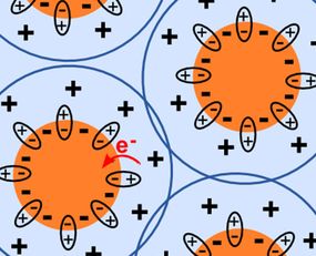
The systematic doping of organic semiconductors with organic or inorganic materials is one of the most important possibilities to influence their electronic properties. Changing the free charge carrier concentration is the key to the optimization of buffer or injection layers of organic devices. Our research focuses on the clarification of doping mechanisms, especially on doping efficiency and doping limit. Another research topic is the relationship between electronic and morphologic properties of doped layers.
Correlation of Electric Device Effects and Electronic Material Properties in OLEDs
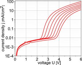
The topic of this project is to develop a general understanding of the origin of some effects observed in IV (current / voltage) and CV (capacitance / voltage) curves of OLED devices. Here, a correlation between the microscopic structural molecular properties, the electronic material and interface properties and their consequence on the macroscopic electric device behavior shall be depicted. For this, selected parts of the device structures are transferred to defined model systems which allows a detailed investigation of relevant aspects. Furthermore, drift-diffusion simulations help to establish a link between electronic and electric properties.
Interface Modifications for Organic Electronics
Designing electronic contact properties of inorganic / organic and organic / organic hetero contacts is one of the key techniques for highly efficient devices. Here, we use self assembling monolayers for a defined tuning of substrate work functions and wetting properties. Our research focuses on a correlation of molecular dipoles and electronic interface alignments as well as contact potentials of selected systems.

X-Ray Photoemission Spectroscopy (XPS)
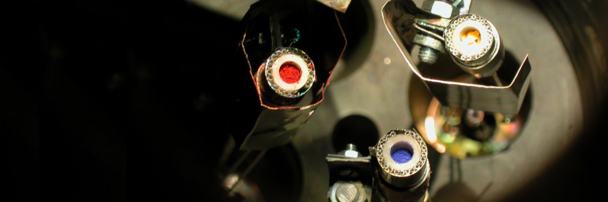
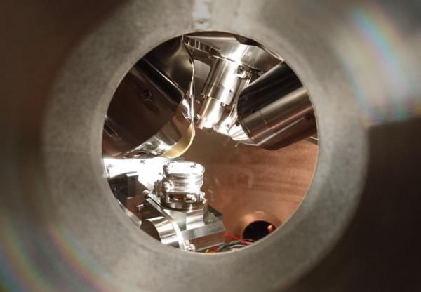
X-ray photoelectron spectroscopy (XPS) allows chemical and electronic investigations of surfaces and interfaces. Therefore, the sample surface is irradiated with monochromated x-rays. The emitted photoelectrons are detected energy dispersively. Due to their small inelastic mean free path in solids XPS is an extremely surface sensitive method. Chemical information given by XPS are the element distributions and their stoichiometry as well as element oxidation states. At InnovationLab we use a "VersaProbe 5000" from Ulvac-Phi equipped with a monochromatic aluminum x-ray tube and a concentric hemispherical analyzer. For in situ analysis it is connected to an integrated UHV system equipped with several evaporation chambers and a glovebox for liquid phase preparation.
UV Photoemission Spectroscopy (UPS)
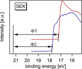
Ultra-violet photoemission spectroscopy (UPS) allows the determination of electronic surface and interface properties. Here, a helium discharge lamp is used to provide excitation light. The method is especially suited for valence electron spectroscopy. Using UPS, the Fermi level position as well as electric surface potentials can be determined by quantifying ionization energies and work functions. In the case of a gradual material deposition on substrates typical mechanisms of contact formation can be investigated, e.g. charge transfers and potential distributions around the contact (band bending and interface dipole). Furthermore, UPS allows the determination of electronic barrier heights at interfaces.
Kelvin Probe
As complementary method to UPS the Kelvin probe is also able to measure the work function and electric surface potentials. In contrast to UPS which uses UV light as excitation source the Kelvin probe works completely contactless using a periodic oscillating metallic mesh. This prevents a possible thermodynamic non-equilibrium situation caused by the UPS light irradiation. However, the work function cannot be quantified absolutely but only relative to a standard material.
PhD Students

Master & Bachelor

Alumni
- Dr. Patrick Reiser
- Dr. Florian Ullrich
- Dr. Eric Mankel
- Dr. Maybritt Münch
- Dr. Paula Connor
- Dr. Julia Maibach
- Sebastian Stolz
- Martin Schwarze
- Marc Hänsel